 Part One Outline
- Introduction
- A simple guide to Cost-Effective Solar Panel Manufacturing & Fabrication
- 3 Types of Panels
- Crystalline Silicone
- Perovskite
Introduction
In this three part blog series we explore what it means to manufacture solar panels. For nearly 40 years Re:Build Optimation has been a leading expert in nearly all of the individual aspects of manufacturing, including roll to roll web based processes. From thin film web technologies, to welding and fabrication, to industrial automation and even glass conveyance and handling. Now that we’re a proud part of the Re:Build Manufacturing family, our partner companies in the Re:Build Ecosystem bolster our strength and make Re:Build Manufacturing a valuable resource for starting and/or scaling solar panel and photovoltaic (PV) manufacturing.
Part one of this blog digs into three anchor types of solar panels that exist in the PV industry. It also explores the exciting possibilities of a future with Perovskite Solar Cells. This section shares about both the chemical makeup and design of the products and some of their pros and cons.
Part two is an explication of a fairly standard manufacturing process as the industry stands today. This is an excellent first pass to learn about the steps in manufacturing a solar panel and great fodder for eventual brainstorming and planning for your eventual projects that involve PV/Solar.
Part three is likely the most exciting part – Roll to Roll (Web) Manufacturing of Solar Cell Technology. The speed with which we can create product in a continuously moving, roll-to-roll manufacturing environment is typically a force multiplied advance in manufacturing. Perovskite technology, coated in line on a web, is a gateway to a future in solar that is high efficiency at low cost.
A Simple Guide to Cost-Effective Solar Panel Manufacturing and Fabrication
Solar energy is one of the most exciting ways to power our homes and businesses, but it’s a bit more complex than just slapping some panels on your roof. In this article, we’ll look at how solar panels are made, from the raw materials all the way to the end product.
According to the Solar Industry Research Data, In the last decade alone, solar has experienced an average annual growth rate of 33%.
It’s obvious that the goal for all engineers is to produce a high-quality product with a cost-efficient process. And the truth is, proper cell engineering can yield 2X electrical efficiency and be much more cost-effective!
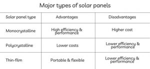
There are three main types of solar panels currently available on the market:
- Thin film solar panels
- Monocrystalline solar panels
- Polycrystalline solar panels
The solar panel manufacturing industry moves at a rapid pace. Information about the latest solar panel production technologies and processes is readily available from various sources.
However, where do you start? What are the latest solar industry trends? How can you be proactive and cost-effectively align your technology investments with anticipated market directions?
Before answering these questions, you’ll need a simple guide to a cost-effective solar panel manufacturing and fabrication process.
This guide is divided into three parts: Thin-film, Monocrystalline, and Polycrystalline cells. When talking about solar panels, these are the three most common types that you’ll see on the market. We’ll begin this discussion by talking about thin-film solar panels.
While thin-film solar panels may not be cost-effective in the short run, they are a viable option for anyone who is concerned about the environment. Silicon-based thin solar panels are usually placed on the roofs of houses because of their heavier weight. In fact, these panels account for almost 70 percent of the world’s thin-film solar panels production. These panels provide high efficiency and power rates when compared to other thin films.
Thin-film solar panels are often made from cadmium telluride (CdTe). It’s highly cost-effective and has been used by the industry since 2001. Most CdTe solar cells are produced using a combination of polycrystalline silicon (PEC) and monocrystalline silicon starting materials. This type of thin-film panel has a layer of CdTe between transparent conducting layers to help capture the sunlight, converting it into usable electricity. This type also has top glass layer protection.
CdTe is often used in conjunction with silicon-based photovoltaic panels and utilizes module technology. However, CdTe has a lower efficiency than crystalline silicon (the most widely used solar panel) but offers a much lower production cost.
When you begin to look at solar panels, one of the factors that you need to consider when making a purchasing decision is the cost of manufacturing. Many solar panel manufacturers don’t like to discuss their manufacturing costs because it can give their competition a competitive advantage. To get around this, many manufacturers have been using third-party sources for their data.
Manufacturing solar panels are typically done in a two-step process. Lithium-based solar panels are made by applying a conductive polymer coating to the glass before it’s cut into wafers. This can be accomplished with an electrodeposition method which uses large copper electrodes and constant voltage (1.7V) to consolidate the conducting polymer layer.
A spray-on technique is also used whereby fine glass particles are sprayed onto the surface of a solution, such as water or propylene carbonate, then dried and heated to 650 Celsius for half an hour. Once the surface is ready for use, photovoltaic glass wafers are added to a vacuum chamber where they will spend at least 24 hours being coated with an anti-reflective layer; a partition layer containing titanium dioxide along with other materials like cobalt oxide, oxygen, and selenium; and finally one or more layers of Copper Indium Gallium Selenide (CIGS) photovoltaic material between the conductive electrodes at the bottom of the chamber which are attached to a power supply. At this point, any remaining air bubbles are removed from the wafer, leaving what is now considered a photovoltaic module. CIGS are proven to achieve 22.8% efficiency compared to crystalline silicon wafer based solar cells.
Crystalline Silicon
The growth of solar power over the last decade has been remarkable. But what are solar panels made of and how are they assembled? The three basic building components of a photovoltaic (PV) solar panel are:
- Silicone
- Solar cells
- Glass
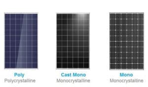
They differ in the types of materials used for cell structure manufacturing: mono silicon, polysilicon, and amorphous silicon (AnSi).
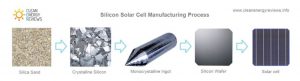
The majority of solar panels are made of silicon wafers. According to LG, silicon makes up 30% of the earth’s crust. Silicon is second to oxygen for availability on the planet.
Solar panels are created by crystalline silicon (i.e. Silicon solar cells). Silicon solar cells have existed since 1954 when the first silicon solar cell was created by an American named Russell Ohl. These cells were made of high purity crystal Si, which is relatively expensive to make and assemble. Nevertheless, these very first Silicon solar panels had an efficiency of 4% or 5%. Today they can reach 19% to 21% efficiency.
Crystalline silicon is sliced into a few millimeter thin wafers to create solar cells that are then cut to shape and polished. Combined, it will create electricity through photons, the so-called particles of lights.
The most efficient type of highly available silicon wafers is monocrystalline. This is due to the fact that it has a higher purity and uniform composition which makes them more efficient in converting light into electric current. They are made using the well-known Czochralski process. This process is more energy-intensive compared to polycrystalline and therefore more expensive to produce.
Polycrystalline wafers are the product of a series of purification processes and a final melting furnace. The material is first purified into crystal grains and then melted down to form a single crystal boule which is then sliced into wafers. Mono wafer cells are cast into silicon ingots, tempered, and sliced into wafers.
Producing silicon-based solar panels requires different steps as it requires many other materials to produce silicon-based solar panels. In manufacturing solar panels, precision is also a very important element, and highly required throughout the whole process. Although many automation has simplified solar panel manufacturing and fabrication process (which increases the affordability of the solar panels), some of the processes still have to be operated by human operators/technicians.
The below image shows us the basic materials that are used in making solar panels.
There are 6 main components in the construction of a typical solar panel:
- Aluminum Frame protects the edges of the panel. It also provides a solid structure that makes it possible to mount the panel in a certain position.
- Tempered glass that protects cells from external hazards. It’s around 3 to 4 mm thick. It is safer than standard glass because even broken tempered glass shatters into tiny fragments rather than sharp pieces that can damage the cell even more.
- Encapsulant: EVA (ethylene vinyl acetate) is a specially designed polymer highly transparent (plastic) layer used to encapsulate the cells and hold them in position during manufacture. It can be made by polymerizing ethylene and vinyl acetate in a tubular reactor from which it can be cast into thin sheets in the same way as polythene film. This is an important step because it will make the finished panels more durable, stiffer, lighter, and resistant to stress cracking.
- Solar cells: solar panel performances are determined by cell types and silicon characteristics. The two main type consists of monocrystalline and polycrystalline silicon.
- Backsheet. A backsheet is an indispensable part of a photovoltaic module or solar cell. Its job is to hold the various layers together to form the final product while providing electrical insulation, protection from moisture and UV exposure, and protection from mechanical damage.
- Junction box: A junction box is needed to securely attach the cables required to interconnect the panels. The junction box also serves as a conduit for wires running from the array that is routed elsewhere in the house.
Amidst all the innovative solar technologies, there are also panels that can receive solar energy from both sides – bifacial panels. It uses a rear glass panel instead of a polymer backsheet. A bifacial module differs from its monofacial counterpart with the presence of a rear-side metallic glass panel. This panel is electrically and thermally connected to the front side module. Arrays that utilize these panels allow energy to be harnessed both at the front and back sides (both sides can be solar). Additionally, this technology helps in lowering the general level of reflected light (and hence increases efficiency) since each module is higher up in front of other modules.
Perovskite: the New Kid on the Block
The new thin film material to promise low cost photovoltaic manufacturing and the potential of high-efficiency is Perovskite. Technically this material is any solar cell made of a crystalline structure equivalent to the same structure as Calcium Titanium Oxide. Use of these cells is much the same as a traditional solar cell – put it in the sun. The promise of 20% or greater efficiency matched with low cost is wonderful but the design potential for this product is equally exciting.
Perovskite cells are best made in a web handling process where thin films are processed via web conveyance in a “solution processing” procedure. The substrates that are coated with Perovskite crystal layers remain flexible and thin enough to present great opportunities. These opportunities include:
- Translucence: A panel made of Perovskite Solar Cells can have multiple active layers.
- Weight Reduction: Modern panels are thick and heavy. Future panels may be much lighter.
- Architectural Integration: Most panels today sit on top of their host – like a residential roof or a mounting pole in a commercial solar array. Future applications may include window tint or other integration into building materials.
- Cross-Technology Integration: A Perovskite panel could be applied over a modern PV panel to add new layers of efficiency. Instead of replacing the old panel it could enhance it while allowing sun to penetrate through and still affect the existing panel. Two PV technologies operating concurrently would be a massive efficiency boost for older tech.
Re:Build Optimation has the skills and the legacy of knowledge to create any type of PV currently available and we are poised to take great advantage of the new Perovskite tech. While this technology is not fully commercialized we see it coming quickly and are thrilled with the massive opportunities it has for the solar power industry. We know it has the potential to greatly enhance green energy solutions for all people.
This concludes Part One of this two part series. Take a moment, if you will, to marvel with us at how one of the most plentiful and seemingly common items on the planet, silica sand, is the bedrock material which allows we humans to harness the power of the sun.
Contact Us
Form located in the contact us page